
In this article, I will present the challenges and the solution to capturing images using the most under-powered microcontroller in the STM32F4 series. The article will go into explaining the reason why we are doing this, an alternative solution, the works of other people trying to do the same, and our solution. I've filled the article with several small remarks that I think would be helpful to people who want to use OV7670 or to connect it to STM32.
Disclaimer: I'm technically a web developer so I may lack expertise and get some of the detail wrong. Furthermore, I wrote this one year after it was done, so I might misremember some details.
Prelude
In my university's 2nd year Embedded System Lab course, the course's final assignment is to build a device that
- Can connect to WiFi
- Uses STM32F401RE Nucleo-64 boards
- Have at least two peripheral
It can be anything: an automatic trash can, a door lock, an air quality tracker. However, some of the student might think that they need a camera, which is completely fine, but some of them, like me, might think that the best way to do it is to buy a standalone camera board, which is a pretty horrible idea as I will explain shortly.
Stop here and just buy an integrated solution
Now that several of my year's camera boards end up in the course's free-item stash, I've heard that some of the current year's students are trying to use them. I highly recommend them to just buy an integrated solution such as an ESP32-CAM board, which comes with a camera attached, and various libraries and example applications that can be built upon. For the price of 350 THB (just within the project rule). This can save you so much time.
What's the problem?
There are several challenges to integrating an OV7670 camera module with an STM32F401RE Nucleo64 board. Some of the major problems are as followed:
OV7670 outputs a high-speed video signal
First, I would like to mention that there are two variants of OV7670 camera boards: One with FIFO and one without FIFO. As pictured below.
Capturing an image generates a lot of bits, which must be captured quickly to avoid distortion. The FIFO variant contains a FIFO chip, which will store the captured frame and allows us to extract the frame data at our own pace. However, the FIFO variant cost more than an ESP32-CAM. So you probably end up with the non-FIFO variant, which requires us to capture 8-bits-wide data at the speed of 24 MHz. High-speed signals are hard to capture and invite all kinds of wiring problems. The sanest way I've seen is to handle it with an FPGA (See this list of cool FPGA Camera projects from MIT 6.111 course).
STM32F401RE is severely under-powered
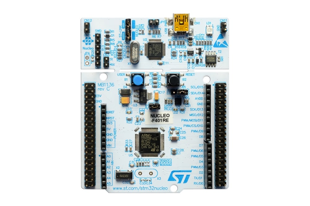 |
STM32 Nucleo-64 board (Photo: ST)
|
If we take a look at the STM32F4 series comparison charts. We can see that STM32F401RE has the lowest performance of the entire series. With the clock speed of 84 MHz, this leaves us with a little room to capture each byte from the camera. And with only 96KB of RAM, storing image data can be difficult. Additionally, being an access-line product, it lacks dedicated DCIM hardware for capturing video signals.
Is it actually possible?
First, we need to do some research in order to determine if it is possible or not? (spoiler: It does! That's why we are reading this)
- AdaFruit's Implementation.
- Support Adafruit Grand Central M4. A quite powerful chip.
- Contains a dedicated Parallel capture controller for capturing video.
- FPGA
- Use BASYS3 FPGA.
- It's an FPGA so processing this signal is not a problem at all.
- Arduino UNO
- Arduino can do it! They read from GPIO and then immediately push it through serial.
- This one pushes it through a TFT display
- STM32F4 Discovery
- This has the closest hardware to us. It's an STM32F4 Series with double the amount of RAM and a DCMI.
We can see a trend that most implementations have one of the following properties:
- Fast signal processing chip (eg. FPGA)
- Signal Passthrough
- Have video capture hardware
Our requirement precludes the 1st option. For the 2nd option, We must store the signal in memory because we have to transmit it over WiFi, so we can't use this option. Which left us with the final option of trying to emulate the video capture hardware with what we have. In the rest of this article, I will describe this approach.
Helpful Reading
This document will only address the specifics of integrating OV7670 with STM32F401RE. So anything else is omitted.
Writing a camera driver from scratch requires us to read the following documents:
Implementation
Solution Overview: Emulating DCMI with GPIO DMA
 |
Interfacing with OV7670
|
To capture the high-bitrate video signal, we decided to use a combination of timers and DMA to quickly moves the input data to memory. Using DMA frees up the CPU and allows us to service other peripherals during image capturing. (In hindsight, Bit-banging GPIO might work too because capturing an image is not really a bottleneck)
The following section will describe the steps of realizing the design above.
Generating XCLK: Under-clocking and PLL
OV7670 requires an external clock signal (XCLK) to function, not just for image output, but also during camera configuration. Since the OV7670's input voltage is not the same as the MCU's output voltage, we need a voltage divider. For output, direct connections work just fine.
Remark: Low XCLK voltage can prevent the camera from working. Ensure
that the module does output PCLK (Pixel Clock) signal after receiving
XCLK.
To give us maximum headroom, we will generate the almost lowest possible XCLK frequency of 10.5 MHz. This should slow down the output the PCLK and thus the pixel bitrate.
Remark: Going below the 10 MHz datasheet limit can result in poor image quality and general instability
To further reduce the data output rate. We can set the camera's register to downscale the clock by 32 times. Additionally, we found that enabling 4x PLL configuration improved the image quality.
Code: TIM initialization snippet, TIM PWM Start Snippet
Configuring the camera using SCCB via I2C
The datasheet introduces the SCCB protocol for configuring the camera. We can see that it is just a modified I2C protocol, so we can just use HAL I2C. Although HAL I2C seems to have a trouble reading the registers, likely due to SCCB not sending ACK bits, we can just disable acknowledgment checking in I2C. Additionally, I found that 100KHz speed seems to work well.
 |
Example of SCCB Transmission. Notice the lack of ACK (Photo: SCCB Reference)
|
Remark: STM32F4 I2C comes with an internal pull-up. No external pull-up resistor needed
Remark: Wiring issues can cause SCCB to freeze in both STM32 and OV7670. I
implemented an I2C soft-reset in the code snippet below. However, some
cases may require power cycling of OV7670 and/or STM32.
We can now set the register to an appropriate value. Please see the reference and the code snippet below for the register values used.
Remark: The undocumented reserved registers must be configured.
Otherwise, the image will look sepia and takes a very long time to
resolve. The register values are taken from Linux's OV7670 driver
Code: I2C initialization snippet, Reading and Writing SCCB using STM32's I2C, Registers Values
Fitting an image inside the RAM
We use the smallest image size preset (QCIF) to allow the image to fit inside the RAM. At 2 bytes/pixel with the dimension of 176 x 144, we have that the image size will be ~50KB which fits inside 96KB RAM. The resulting output is actually slightly larger than QCIF for some reason.
Remark: Documentation regarding custom image size settings seems to be lacking, so I just use preset size.
Catching pixels with DMA and a chain of timers
Setting up the PIXCLK trigger and DMA
We want to trigger a DMA request during the rising edge of the Pixel Clock (PIXCLK). To do that, we connect the PIXCLK wire to TIM1_CH1, turn on Input Capture for the channel, and then enable the trigger for sending a DMA request on input capture. We configure DMA to transfer the data from GPIO Register to Memory. The transfer should be in the circular mode to continuously capture the image as DMA have significant overhead to start and stop, transfer can still be controlled by starting and stopping the timer which originates DMA requests.
 |
| DMAs' bus connection (Photo: STM32 Reference) |
Remark: Incompatible TIM, DMA, and GPIO can result in DMA transfer errors. Lookup the GPIO's Bus in the datasheet's Register Boundary Addresses Table. Then ensure that DMA can access the peripheral by looking up Bus Matrix Diagram. Finally, ensure that there is a DMA channel that can be triggered by the Timer. Ensure that DMA's destination buffer does not violate DMA constraints.
Code: TIM1 PIXCLK Capture Setup, DMA Setup
Setting up HSYNC and VSYNC timer and Synchronize it with PIXCLK timer
We set up the TIM3 timer to count the number of pixels received by syncing it with the PIXCLK timer.
Remark: Capturing sync signals is necessary when the wiring is unreliable. Without sync, a corrupted signal can lead to cascading shifting of the image's pixel.
To generate trigger output at every PIXCLK, we set up the PIXCLK TIM (TIM1) in slave mode to use TI1FP1 (Input Capture) signal as a trigger and set TIM1 to slave mode reset to reset its counter at every capture. We then set TIM1's master mode to output TGRO at every reset event.
 |
TIM1's available MUXes (Photo: STM32 Reference)
|
We then clock TIM3 by TIM1's TGRO by setting it in external clock mode. See the timer connection table for choosing an appropriate channel.
 |
TIMx's timer connection (Photo: STM32 Reference)
|
Finally, connect HSYNC and VSYNC to TIM3 and set up input capture mode with interrupt.
Remark: I don't recall why I did not combine TIM3 with TIM1
Code: Sync Timer (TIM3) Setup
Capturing the image
Now that we have everything ready. We can now start to capture an image. We use the following steps to capture a single frame:
- Start TIM1 and TIM3
- Start circular DMA
- When the VSYNC interrupt is triggered, record the DMA's current writing offset as the start of the frame. (Use NDTR. Note that NDTR counts down)
- Every HSYNC interrupt, record the current writing offset as the start of the line
- Once another VSYNC is received, stop TIM1 and TIM3
- Reconstruct the image using VSYNC and HSYNC offset recorded
Remark: Wiring issues can cause the image to be corrupted. We can fix this by repeating the capture process until the number of HSYNC lines and the distance between each hsync looks reasonable.
Code: Capture Code
Result
Now, transfer the buffer to a PC and display it. Here's an image that I've captured:
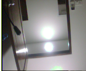 |
Image Output
|
After all this, our MCU probably run out of all its pins. As can be seen in the picture below:
|
| All the wirings |
|
|
The process of capturing an image is really quick, because if it isn't, then our image will get distorted. The slowest part for us is sending the image over UART to be displayed on the PC.
Extra: Sending an image to ESP8266
To transfer an image over WiFi through ESP8266. Since the image is bigger than the ESP8266's RAM, one must write a streaming HTTP client to receive the image through SPI. Additionally, jumper wires are not reliable and prone to burst error, so we must build an error-tolerant protocol with backpressure to fix this (I do not recommend using that part of my code for that, It is really slow and badly designed).
Conclusion
We have demonstrated that capturing an image with the lowest-tier STM32F4 MCU is indeed possible. However, the image resolution is poor, we run out of pins, and it took a lot of effort to make it work. I hope that this article helps dissuad people from doing this or help them make it work if they want to.
<END>


Comments
Post a Comment